搜索附件  
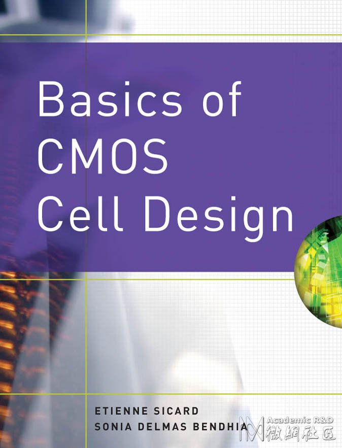
头雁微网 附件中心 专业技术 微波工程 Basics of CMOS Cell Design - 0071488391: Basics of CMOS Cell Design - 0071488391.jpg
板块导航
附件中心&附件聚合2.0
For Discuz! X3.5 © hgcad.com

Basics of CMOS Cell Design - 0071488391: Basics of CMOS Cell Design - 0071488391.jpg


Basics of CMOS Cell Design - 0071488391:
Copyright © 2007 by The McGraw-Hill Companies, Inc. Manufactured in the United States of America. Except as permitted under the
United States Copyright Act of 1976, no part of this publication may be reproduced or distributed in any form or by any means, or stored
in a database or retrieval system, without the prior written permission of the publisher.
0-07-150906-2
The material in this eBook also appears in the print version of this title: 0-07-148839-1.
All trademarks are trademarks of their respective owners. Rather than put a trademark symbol after every occurrence of a trademarked
name, we use names in an editorial fashion only, and to the benefit of the trademark owner, with no intention of infringement of the
trademark. Where such designations appear in this book, they have been printed with initial caps.
McGraw-Hill eBooks are available at special quantity discounts to use as premiums and sales promotions, or for use in corporate training
programs. For more information, please contact George Hoare, Special Sales, at george_hoare@mcgraw-hill.com or (212) 904-4069.
TERMS OF USE
This is a copyrighted work and The McGraw-Hill Companies, Inc. (“McGraw-Hill”) and its licensors reserve all rights in and to the
work. Use of this work is subject to these terms. Except as permitted under the Copyright Act of 1976 and the right to store and retrieve
one copy of the work, you may not decompile, disassemble, reverse engineer, reproduce, modify, create derivative works based upon,
transmit, distribute, disseminate, sell, publish or sublicense the work or any part of it without McGraw-Hill’s prior consent. You may use
the work for your own noncommercial and personal use; any other use of the work is strictly prohibited. Your right to use the work may
be terminated if you fail to comply with these terms.
THE WORK IS PROVIDED “AS IS.” McGRAW-HILL AND ITS LICENSORS MAKE NO GUARANTEES OR WARRANTIES AS
TO THE ACCURACY, ADEQUACY OR COMPLETENESS OF OR RESULTS TO BE OBTAINED FROM USING THE WORK,
INCLUDING ANY INFORMATION THAT CAN BE ACCESSED THROUGH THE WORK VIA HYPERLINK OR OTHERWISE,
AND EXPRESSLY DISCLAIM ANY WARRANTY, EXPRESS OR IMPLIED, INCLUDING BUT NOT LIMITED TO IMPLIED
WARRANTIES OF MERCHANTABILITY OR FITNESS FOR A PARTICULAR PURPOSE. McGraw-Hill and its licensors do not
warrant or guarantee that the functions contained in the work will meet your requirements or that its operation will be uninterrupted or
error free. Neither McGraw-Hill nor its licensors shall be liable to you or anyone else for any inaccuracy, error or omission, regardless
of cause, in the work or for any damages resulting therefrom. McGraw-Hill has no responsibility for the content of any information
accessed through the work. Under no circumstances shall McGraw-Hill and/or its licensors be liable for any indirect, incidental, special,
punitive, consequential or similar damages that result from the use of or inability to use the work, even if any of them has been advised
of the possibility of such damages. This limitation of liability shall apply to any claim or cause whatsoever whether such claim or cause
arises in contract, tort or otherwise.
DOI: 10.1036/0071488391
Preface vii
Acknowledgments ix
Abbreviations and Symbols xv
1. Introduction 1
1.1 General Trends 1
1.2 The Device Scale Down 5
1.3 Frequency Improvements 5
1.4 Layers 6
1.5 Density 8
1.6 Design Trends 10
1.7 Market 11
1.8 Conclusion 11
References 11
Exercises 12
2. The MOS Devices and Technology 13
2.1 Properties of Silicon 13
2.2 N-type and P-type Silicon 16
2.3 Silicon Dioxide 18
2.4 Metal Materials 19
2.5 The MOS Switch 20
2.6 The MOS Aspect 23
2.7 MOS Layout 25
2.8 Dynamic MOS Behaviour 32
2.9 The Perfect Switch 38
2.10 Layout Considerations 41
2.11 CMOS Process 44
2.12 Conclusion 48
References 48
Exercises 48
3. The MOS Modelling 51
3.1 Introduction to Modelling 51
3.2 MOS Model 1 53
3.3 MOS Model 3 57
3.4 The BSIM4 MOS Model 66
3.5 Specifi c MOS Devices 80
3.6 Process Variations 87
For more information about this title, click here
3.7 Concluding Remarks 90
References 91
Exercises 91
4. The Inverter 93
4.1 Logic Symbol 93
4.2 CMOS Inverter 94
4.3 Inverter Layout 95
4.4 Inverter Simulation 104
4.5 Power Consumption 111
4.6 Static Characteristics 114
4.7 Random Simulation 118
4.8 The Inverter as a Library Cell 120
4.9 3-State Inverter 122
4.10 All nMOS Inverters 125
4.11 Ring Oscillator 127
4.12 Latch-up Effect 133
4.13 Conclusion 134
References 134
Exercises 135
5. Interconnects 137
5.1 Introduction 137
5.2 Metal Layers 137
5.3 Contact and Vias 139
5.4 Design Rules 142
5.5 Capacitance Associated with Interconnects 146
5.6 Resistance Associated with Interconnects 153
5.7 Signal Transport 157
5.8 Improved Signal Transport 164
5.9 Repeaters for Improved Signal Transport 167
5.10 Crosstalk Effects in Interconnects 169
5.11 Antenna Effect 173
5.12 Inductance 176
5.13 Conclusion 179
References 179
Exercises 180
6. Basic Gates 182
6.1 Introduction 182
6.2 Combinational Logic 182
6.3 CMOS Logic Gate Concept 184
6.4 The NAND Gate 185
6.5 The AND Gate 202
6.6 The NOR Gate 204
xii Contents
6.7 The OR Gate 207
6.8 The XOR Gate 208
6.9 Complex Gates 214
6.10 Multiplexor 218
6.11 Shifters 227
6.12 Description of Basic Gates in Verilog 229
6.13 Conclusion 231
References 231
Exercises 231
7. Arithmetics 233
7.1 Data Formats 233
7.2 The Adder Circuit 236
7.3 Adder Cell Design 238
7.4 Ripple-carry Adder 247
7.5 Signed Adder 253
7.6 Fast Adder Circuits 254
7.7 Substractor Circuit 258
7.8 Comparator Circuit 260
7.9 Student Project: A Decimal Adder 262
7.10 Multiplier 267
7.11 Conclusion 272
References 272
Exercises 273
8. Sequential Cell Design 274
8.1 The Elementary Latch 274
8.2 RS Latch 275
8.3 D Latch 282
8.4 Edge-trigged D Register 288
8.5 Clock Divider 295
8.6 Synchronous Counters 299
8.7 Shift Registers 301
8.8 A 24-hour Clock 303
8.9 Conclusion 307
References 307
Exercises 307
9. Analog Cells 309
9.1 Resistor 309
9.2 Capacitor 314
9.3 The MOS Device for Analog Design 321
9.4 Diode-connected MOS 324
9.5 Voltage Reference 326
9.6 Current Mirror 331
Contents xiii
9.7 The MOS Transconductance 335
9.8 Single Stage Amplifi er 336
9.9 Simple Differential Amplifi er 345
9.10 Wide Range Amplifi er 354
9.11 On-chip Voltage Regulator 357
9.12 Noise 359
9.13 Conclusion 361
References 361
Exercises 361
10. Conclusion 363
Appendices
A. Design Rules 364
A.1 Lambda Units 364
A.2 Layout Design Rules 365
A.3 Pads 368
A.4 Electrical Extraction Principles 368
A.5 Node Capacitance Extraction 369
A.6 Resistance Extraction 372
A.7 Simulation Parameters 373
A.8 Technology Files for Dsch 376
B. Microwind Program Operation and Commands 378
B.1 Getting Started 378
B.2 List of Commands in Microwind 379
C. Dsch Logic Editor Operation and Commands 403
C.1 Getting Started 403
C.2 Commands 403
D. Quick Reference Sheet 413
D.1 Microwind Menus 413
D.2 Microwind Simulation Menu 416
D.3 Dsch Menus 417
D.4 List of Files 419
D.5 List of Measurement Files 419
Glossary 422
Index 424
Software Download Information 428
Authors’ Profi les 429


感谢楼主分享
谢谢楼主了
感谢楼主分享,感谢微网推荐
谢谢楼主分享
谢谢提供资料
看一看再说
xuexiele
谢谢提供资料{:soso_e100:}
Basics of CMOS Cell Design - 0071488391: Basics of CMOS Cell Design - 0071488391.jpg
客服中心 搜索
关于我们
关于我们
关注我们
联系我们
帮助中心
资讯中心
企业生态
社区论坛
服务支持
资源下载
售后服务
推广服务
关注我们
官方微博
官方空间
官方微信
返回顶部