搜索附件  
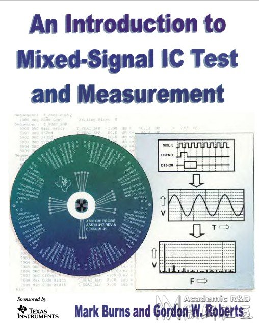
头雁微网 附件中心 专业技术 微波工程 An_introduction_to_mixed_signal_ic_test_and_measurement: An_introduction_to_mixed_signal_ic_test_and_measurement.part2.rar
板块导航
附件中心&附件聚合2.0
For Discuz! X3.5 © hgcad.com

An_introduction_to_mixed_signal_ic_test_and_measurement: An_introduction_to_mixed_signal_ic_test_and_measurement.part2.rar


An_introduction_to_mixed_signal_ic_test_and_measurement:

Oxford University Press
Oxford New York
Athens Auckland Bangkok Bogota Buenos Aires Calcutta
Cape Town Chennai Oar es Salaam Delhi Florence Hong Kong Istanbul
Karachi Kuala Lumpur Madrid Melbourne Mexico City Mumbai
Nairobi Paris Sao Paulo Shanghai Singapore Taipei Tokyo Toronto Warsaw
and associated companies in
Berlin !badan
Copyright @ 2001 by Texas Instruments, blcorporated
Published by Oxford University Press, Inc.
198 Madison Avenue, New York, New York, 10016
http://www.oup-usa.org
Oxford is a registered trademark of Oxford University Press
All rights reserved. No part of this publication may be reproduced,
stored in a retrieval system, or transmitted, in any form or by any means,
electronic, mechanical, photocopying, recording, or otherwise,
without the prior permission of Oxford University Press.
Library of Congress Cataloging-in-Publication Data
Bums, Mark, 1962-
An introductiont o mixed-signal IC test and measuremenIt Mark Bums, GordonR oberts
p. cm. - (Oxfords eriesin electricaal ndc omputeern gineering)
Includes bibliographical references and index.
ISBN 0-19-514016-8
I. Integrated circuits-Testing. 2. Mixed signal circuits-Testing. I. Roberts, Gordon
W., 1959- II. Title. III. Series
TK7874 .B825 2000
621.38IS-dc2I
00-042770
PREFACE xvii
1.1 MIXED-SIGNAL CIRCUITS 1
1.1.1 Analog, Digital, or Mixed-Signal? 1
1.1.2 Common Types of Analog and Mixed-Signal Circuits
1.1.3 Applicationso f Mixed-SignaCl ircuits 3
1.2 WHY TEST MIXED-SIGNAL DEVICES? 5
1.2.1 The CMOS FabricationP rocess 5
1.2.2 Real-WorldCircuits 5
1.2.3 What Is a Test Engineer? 8
1.3 POST-SILICON PRODUCTION FLOW 10
1.3.1 Test and Packaging 10
1.3.2 Characterizatiovne rsusP roductionT esting 11
1.4 TEST AND DIAGNOSTIC EQUIPMENT 11
1.4.1 Automated Test Equipment 11
1.4.2 Wafer Probers 13
1.4.3 Handlers 13
1.4.4 E-Beam Probers 14
1.4.5 FocusedIo n BeamE quipment 15
1.4.6 Forced-TemperatuSrey stems 15
1.5 NEW PRODUCT DEVELOPMENT 16
1.5.1 ConcurrenEt ngineering 16
1.6 MIXED-SIGNAL TESTING CHALLENGES 17
1.6.1 Time to Market 18
1.6.2 Accuracy,R epeatabilitya, ndC orrelation 18
1.6.3 ElectromechanicaFli xturingC hallenges 18
1.6.4 Economicso f ProductionT esting 19
Chapter 2: The Test Specification Process
2.1 DEVICE DATA SHEETS 23
2.1.1 Purposeo f a DataS heet 23
2.1.2 Structure of a Data Sheet 24
2.1.3 Electrical Characteristics 27
2.2 GENERATING THE TEST PLAN 31
2.2.1 To Plan or Not to Plan 31
v
vi Contents
2.2.2 Structure of a Test Plan 35
2.2.3 DesignS pecificationvse rsusP roductionT estS pecifications 36
2.2.4 Convertingt he DataS heetin to a Test Plan 37
2.3 COMPONENTS OF A TEST PROGRAM 38
2.3.1 Test Program Structure 38
2.3.2 Test Code and Digital Patterns 38
2.3.3 Binning 40
2.3.4 Test SequencCe ontrol 40
2.3.5 WaveformC alculationsa ndO therI nitializations 41
2.3.6 FocusedC alibrationsa ndD IB Checkers 41
2.3.7 CharacterizatioCn ode 42
2.3.8 Simulation Code 42
2.3.9 "Debuggability" 42
2.4 SUMMARY 43
Chapter 3: DC and Parametric Measurements
3.1 CONTINUITY 45
3.1.1 Purposeo f ContinuityT esting 45
3.1.2 Continuity Test Technique 46
3.1.3 Serial versus Parallel Continuity Testing 48
3.2 LEAKAGE CURRENTS 50
3.2.1 Purposeo f LeakageT esting 50
3.2.2 Leakage Test Technique 50
3.2.3 Serialv ersusP arallelL eakageT esting 51
3.3 POWER SUPPLY CURRENTS 51
3.3.1 hnportanceo f SupplyC urrentT ests 51
3.3.2 Test Techniques 51
3.4 DC REFERENCES AND REGULATORS 52
3.4.1 Voltage Regulators 52
3.4.2 Voltage References 55
3.4.3 Trirnmable References 55
3.5 IMPEDANCE MEASUREMENTS 56
3.5.1 Input hnpedance 56
3.5.2 Output hnpedance 58
3.5.3 Differential hnpedanceM easurements 59
3.6 DC OFFSET MEASUREMENTS 60
3.6.1 VMIDa ndA nalogG round 60
3.6.2 DC TransferC haracteristic(sG ain andO ffset) 60
3.6.3 OutputOffsetVoltage(Vo) 61
3.6.4 Single-EndedD, ifferential,a ndC ommon-ModeO ffsets 62
3.6.5 Input Offset Voltage (V os) 64
3.7 DC GAIN MEASUREMENTS 65
3.7.1 Closed-LoopG ain 65
3.7.2 Open-Loop Gain 68
3.8 DC POWER SUPPLY REJECTION RATIO 71
3.8.1 DC Power Supply Sensitivity 71
3.8.2 DC Power Supply Rejection Ratio 72
Contents vii
3.9 DC COMMON-MODE REJECTION RATIO 72
3.9.1 CMRRofOpAmps 72
3.9.2 CMRR of Differential Gain Stages 75
3.10 COMPARATOR DC TESTS 77
3.10.1 Input Offset Voltage 77
3.10.2 Thresho1dVoltage 78
3.10.3 Hysteresis 78
3.11 VOLTAGE SEARCH TECHNIQUES 79
3.11.1 Binary Searchevse rsusS tepS earches 79
3.11.2 Linear Searches 80
3.12 DC TESTS FOR DIGJTAL CIRCUITS 82
3.12.1 4H/4L 82
3.12.2 VldV/L 82
3.12.3 VaN/VoL 82
3.12.4 IoH/loL 82
3.12.5 IoSHa ndI osLS hortC ircuit Current 82
3.13 SUMMARY 83
Chapter 4: Measurement Accuracy
4.1 TERMINOLOGY 87
4.1.1 Accuracy and Precision 87
4.1.2 SystematicE rrors 88
4.1.3 Random Errors 88
4.1.4 Resolution( QuantizationE rror) 88
4.1.5 Repeatability 89
4.1.6 Stability 90
4.1.7 Correlation 91
4.1.8 Reproducibility 92
4.2 CALIBRATIONS AND CHECKERS 93
4.2.1 Traceability to Standards 93
4.2.2 Hardware Calibration 93
4.2.3 Software Calibration 93
4.2.4 SystemC alibrationsa ndC heckers 96
4.2.5 FocusedIn strumenCt alibrations 97
4.2.6 FocusedD IB Circuit Calibrations 101
4.2.7 DIB Checkers 102
4.2.8 Tester Specifications 103
4.3 DEALING WITH MEASUREMENT ERROR 106
4.3.1 Filtering 106
4.3.2 Averaging 111
4.3.3 Guardbanding 113
4.4 BASIC DATA ANALYSIS 114
4.4.1 Datalogs 114
4.4.2 Histograms 115
4.4.3 Noise, Test Time, and Yield 118
4.5 SUMMARY 120
viii Contents
Chapter 5: Tester Hardware
5.1 MIXED-SIGNAL TESTER OVERVIEW 123
5.1.1 General-PurposTee stersv ersusF ocusedB enchE quipment 123
5.1.2 Generic Tester Architecture 123
5.2 DC RESOURCES 125
5.2.1 General-PurposMeu 1timeters 125
5.2.2 General-PurposVeo ltage/CurrenSt ources 127
5.2.3 PrecisionV oltageR eferenceasn dU serS upplies 128
5.2.4 Calibration Source 128
5.2.5 Relay Matrices 128
5.2.6 Relay Control Lines 130
5.3 DIGITAL SUBSYSTEM 131
5.3.1 Digital Vectors 131
5.3.2 Digital Signals 131
5.3.3 Source Memory 132
5.3.4 Capture Memory 132
5.3.5 Pin Card Electronics 134
5.3.6 Timing andF ormattingE lectronics 136
5.4 AC SOURCE AND MEASUREMENT 139
5.4.1 AC ContinuousW aveS ourcea ndA C Meter 139
5.4.2 Arbitrary Waveform Generators 139
5.4.3 Waveform Digitizers 140
5.4.4 Clocking and Synchronization 141
5.5 TIME MEASUREMENT SYSTEM 141
5.5.1 Time Measurements 141
5.5.2 Time MeasuremenInt terconnects 142
5.6 COMPUTING HARDWARE 143
5.6.1 User Computer 143
5.6.2 Tester Computer 144
5.6.3 Array Processorasn dD istributedD igital SignalP rocessors 144
5.6.4 Network Connectivity 144
5.7 SUMMARY 144
Chapter 6: Sampling Theory
6.1 ANALOG MEASUREMENTS USING DSP 147
6.1.1 Traditionalv ersusD SP-BaseTd estingo f AC Parameters 147
6.2 SAMPLING AND RECONSTRUCTION 148
6.2.1 Use of Samplinga ndR econstructionin Mixed-SignaTl esting 148
6.2.2 Sampling:C ontinuous-Timaen dD iscrete-TimeR epresentation 149
6.2.3 Reconstruction 152
6.2.4 The Sampling Theorem and Aliasing 159
6.2.5 QuantizationE ffects 161
6.2.6 Sampling Jitter 166
6.3 REPETITIVE SAMPLE SETS 170
6.3.1 Finite and Infmite Sample Sets 170
6.3.2 CoherentS ignalsa ndN oncoherenSt ignals 171
Contents ix
6.3.3 Peak-to-RMSC ontroli n CoherenMt ultitones 173
6.3.4 Spectral Bin Selection 175
6.4 SYNCHRONIZATION OF SAMPLING SYSTEMS 179
6.4.1 SimultaneouTs estingo f Multiple SamplingS ystems 179
6.4.2 ATE Clock Sources 181
6.4.3 The Challengeo f Synchronization 183
6.S SUMMARY 184
Chapter 7: DSP-Based Testing
7.1 ADVANTAGES OF DSP-BASED TESnNG 189
7.1.1 ReducedTestTime 189
7.1.2 Separationo f SignalC omponents 189
7.1.3 Advanced Signal Manipulations 190
7.2 DIGITAL SIGNAL PROCESSING 190
7.2.1 DSP and Array Processing 190
7.2.2 Fourier Analysis of Periodic Signals 191
7.2.3 The TrigonometricF ourierS eries 192
7.2.4 The Discrete-TimeF ourierS eries 195
7.2.5 CompleteF requencyS pectrum 205
7.2.6 Time andF requencyD enormalization 210
7.2.7 Complex Form of the DTFS 211
7.3 DISCRETE-TIME TRANSFORMS 213
7.3.1 The Discrete Fourier Transform 213
7.3.2 The Fast Fourier Transform 216
7.3.3 Interpretingt he FFT Output 218
7.4 THE INVERSE FFT 230
7.4.1 Equivalenceo f Time- andF requency-DomaiInn formation 230
7.4.2 Parseval'sT heorem 232
7.4.3 Applications of the Inverse FFT 233
7.4.4 Frequency-DomaiFni ltering 234
7.4.5 Noise Weighting 239
7.5 SUMMARY 240
APPENDIXA.7.1 241
~
Chapter 8: Analog Channel Testing
8.1 OVERVIEW 249
8.1.1 Types of Analog Channels 249
8.1.2 Typeso f AC ParametricT ests 250
8.1.3 Review of Logarithmic Operations 250
8.2 GAIN AND LEVEL TESTS 251
8.2.1 Absolute Voltage Levels 251
8.2.2 Absolute Gain and Gain Error 256
8.2.3 Gain Tracking Error 258
8.2.4 PGA Gain Tests 260
8.2.5 FrequencyR esponse 265
x Contents
8.3 PHASE TESTS 273
8.3.1 PhaseR esponse 273
8.3.2 Group Delay and Group Delay Distortion 278
8.4 DISTORTION TESTS 280
8.4.1 Signal to Hannonic Distortion 280
8.4.2 InteTnlodulatioDn istortion 283
8.5 SIGNAL REJECTION TESTS 284
8.5.1 Common-ModeR ejectionR atio 284
8.5.2 Power Supply Rejection and Power Supply Rejection Ratio 287
8.5.3 Channel-to-ChannCelr osstalk 289
8.5.4 Clock and Data Feedthrough 293
8.6 NOISE TESTS 293
8.6.1 Noise 293
8.6.2 Idle ChanneNl oise 294
8.6.3 Signal to Noise, Signal to Noise and Distortion 296
8.6.4 SpuriousF reeD ynamicR ange 298
8.6.5 Weighting Filters 300
8.7 SIMULA nON OF ANALOG CHANNEL TESTS 304
8.7.1 MATLAB Model of an Analog Channel 304
8.8 SUMMARY 308
Chapter 9: Sampled Channel Testing
9.1 OVERVIEW 315
9.1.1 WhatAreSampledChannels? 315
9.1.2 Exampleso f SampledC hannels 315
9.1.3 Typeso f SampledC hannels 318
9.2 SAMPLING CONSmERATIONS 320
9.2.1 DUT Sampling Rate Constraints 320
9.2.2 Digital SignalS ourcea ndC apture 321
9.2.3 SimultaneouDs AC andA DC ChanneTl esting 326
9.2.4 MismatchedF undamentaFl requencies 330
9.2.5 Undersampling 333
9.2.6 ReconstructionE ffectsi n A WGs,D ACs, andO therS ampled-DatCa ircuits 335
9.3 ENCODING AND DECODING 338
9.3.1 Signal Creation and Analysis 338
9.3.2 Data Formats 339
9.3.3 Intrinsic Errors 344
9.4 SAMPLED CHANNEL TESTS 350
9.4.1 Similarity to Analog Channel Tests 350
9.4.2 Absolute Level, Absolute Gain, Gain Error, and Gain Tracking 351
9.4.3 FrequencyR esponse 356
9.4.4 PhaseR esponse(A bsoluteP haseS hift) 359
9.4.5 Group Delay and Group Delay Distortion 360
9.4.6 Signalt o HarmonicD istortion,I ntermodulationD istortion 360
9.4.7 Crosstalk 361
9.4.8 CMRR 362
Contents xi
9.4.9 PSRandPSRR 362
9.4.10 Signal-to-NoiseR atioa ndE NOB 363
9.4.11 Idle ChanneNl oise 363
9.S SUMMARY 364
Chapter 10: Focused Calibrations
10.1 OVERVIEW 369
10.1.1 Traceability to National Standards 369
10.1.2 Why Are FocusedC alibrationsN eeded? 370
10.1.3 Typeso f FocusedC alibrations 372
10.1.4 Mechanicso f FocusedC alibration 372
10.1.5 Program Structure 375
10.2 DC CALIBRAllONS 376
10.2.1 DC Offset Calibration 376
10.2.2 DC Gain and Offset Calibrations 378
10.2.3 CascadingD C Offseta ndG ain Calibrations 380
10.3 AC AMPLITUDE CALIBRATIONS 382
10.3.1 Calibrating AWGs and Digitizers 382
10.3.2 Low-Level A WG and Digitizer Amplitude Calibrations 389
10.3.3 AmplitudeC alibrationsfo r ADC andD AC Tests 390
10.4 OTHER AC CALIBRATIONS 392
10.4.1 Phase Shifts 392
10.4.2 Digitizer and A WG Synchronization 396
10.4.3 DAC andA DC PhaseS hifts 396
10.4.4 Distortion Tests 396
10.4.5 Noise Tests 397
10.5 ERROR CANCELLATION TECHNIQUES 397
10.5.1 Avoiding Absolute Calibration 397
10.5.2 Gain andP haseM atching 397
10.5.3 Differential Gain and Differential Phase 399
10.6 SUMMARY 400
Chapter 11: DAC Testing
11.1 BASICS OF CONVERTER TESTING 403
11.1.1 Intrinsic Parametervse rsusT ransmissionP arameters 403
11.1.2 Comparisono fDACs andA DCs 404
11.1.3 DACFai1ureMechanisrns 405
11.2 BASIC DC TESTS 405
11.2.1 Code-SpecificP arameters 405
11.2.2 Full-Scale Range 406
11.2.3 DC Gain, Gain Error, Offset, and Offset Error 406
11.2.4 LSB Step Size 409
11.2.5 DCPSS 410
11.3 TRANSFER CURVE TESTS 410
11.3.1 Absolute Error 410
11.3.2 Monotonicity 412
xii Contents
11.3.3 DifferentialNon1inearity 412
11.3.4 Integra1Nonlinearity 416
11.3.5 Partial Transfer Curves 419
11.3.6 Major Carrier Testing 420
11.3.7 OtherS elected-CodTee chniques 423
11.4 DYNAMIC DAC TESTS 424
11.4.1 ConversionT ime (SettlingT ime) 424
11.4.2 Overshooat ndU ndershoot 426
11.4.3 Rise Time and Fall Time 426
11.4.4 DAC-to-DAC Skew 426
11.4.5 Glitch Energy (Glitch Impulse) 427
11.4.6 Clock and Data Feedthrough 428
11.5 DAC ARCHITECTURES 428
11.5.1 ResistiveDividerDACs 428
11.5.2 Binary-WeightedDACs 430
11.5.3 PWMDACs 431
11.5.4 Sigma-DeltaD ACs 433
11.5.5 CompandedD ACs 434
11.5.6 Hybrid DAC Architectures 435
11.6 TESTS FOR COMMON DAC APPLICAnONS 435
11.6.1 DC References 435
11.6.2 Audio Reconstruction 436
11.6.3 Data Modulation 436
11.6.4 Video Signal Generators 436
11.7 SUMMARY 437
APPENDIXA.ll.l 437
Chapter 12: ADC Testing
12.1 ADC TESTING VERSUS DAC TESTING 447
12.1.1 ComparisonofDACsandADCs 447
12.1.2 StatisticalB ehavioro f ADCs 448
12.2 ADC CODE EDGE MEASUREMENTS 454
12.2.1 Edge Code Testing versus Center Code Testing 454
12.2.2 StepS earcha ndB inary SearchM ethods 455
12.2.3 Servo Method 455
12.2.4 Linear RampH istogramM ethod 456
12.2.5 Conversionfr om Histogramsto CodeE dgeT ransferC urves 457
12.2.6 Accuracy Limitations of Histogram Testing 460
12.2.7 Rising Ramps versus Falling Ramps 461
12.2.8 SinusoidaHl istogramM ethod 462
12.3 DC TESTS AND TRANSFER CURVE TESTS 467
12.3.1 DC Gain and Offset 467
12.3.2 INL and DNL 468
12.3.3 Monotonicity and Missing Codes 469
12.4 DYNAMIC ADC TESTS 470
12.4.1 ConversionT ime, RecoveryT ime, and SamplingF requency 470
12.4.2 Aperture Jitter 472
12.4.3 Sparkling 472
Contents xiii
12.5 ADC ARCmTECTURES 473
12.5.1 SuccessivAe pproximationA rchitectures 473
12.5.2 IntegratingA DCs (Dual-Slopea ndS ingle-Slope) 474
12.5.3 Flash ADCs 475
12.5.4 SemiflashA DCs 476
12.5.5P DM (Sigma-DeltaA) DCs 477
12.6 TESTS FOR COMMON ADC APPLICATIONS 479
12.6.1 DC Measurements 479
12.6.2 Audio Digitization 479
12.6.3 Data Transmission 479
12.6.4 Video Digitization 480
12.7 SUMMARY 480
13: DIB Design
13.1 DIB BASICS 483
13.1.1 Purposeo f a DeviceI nterfaceB oard 483
13.1.2 Dffi Configurations 484
13.1.3 Importanceo f GoodD IB Design 486
13.2 PRINTED CIRCillT BOARDS 486
13.2.1 Prototype DIBs versus PCB Dffis 486
13.2.2 PCB CAD Tools 487
13.2.3 Multilayer PCBs 488
13.2.4 PCB Materials 489
13.3 DIB TRACES, SHIELDS, AND GUARDS 490
13.3.1 Trace Parasitics 490
13.3.2 Trace Resistance 490
13.3.3 Trace Inductance 491
13.3.4 Trace Capacitance 496
13.3.5 Shielding 502
13.3.6 Driven Guards 503
13.4 TRANSMISSION LINES 504
13.4.1 Lumped-a ndD istributed-ElemenMt odels 504
13.4.2T ransmissionL ine Termination 508
13.4.3P arasiticL umpedE lements 514
13.5 GROUNDING AND POWER DISTRIBUTION 514
13.5.1 Grounding 514
13.5.2 Power Distribution 516
13.5.3 Power and Ground Planes 517
13.5.4 Ground Loops 518
13.6 DIB COMPONENTS 519
13.6.1D UT Socketsa ndC ontactorA ssemblies 519
13.6.2 Contact Pads, Pogo Pins, and Socket Pins 520
13.6.3 ElectromechanicaRle lays 521
13.6.4 Socket Pins 524
13.6.5 Resistors 525
13.6.6 Capacitors 526
13.6.7 Inductors and Ferrite Beads 528
13.6.8T ransformersa ndP owerS plitters 528
xiv Contents
13.7 COMMON DIB CIRCUITS 530
13.7.1 Local Relay Connections 530
13.7.2 Relay Multiplexers 532
13.7.3 SelectableL oads 533
13.7.4 Analog Buffers (Voltage Followers) 533
13.7.5 InstrumentatioAn mplifiers 534
13.7.6 VMIDR eferenceA dder 535
13.7.7 Current-toV- oltagea ndV oltage-to-CurrenCt onversions 536
13.7.8 Power Supply Ripple Circuits 536
13.8 COMMON DIB MISTAKES 540
13.8.1 Poor Power Supply and Ground Layout 540
13.8.2 Crosstalk 541
13.8.3 TransmissionL ine Discontinuities 541
13.8.4 Resistive Drops in Circuit Traces 541
13.8.5 TesterI nstrumenPt arasitics 541
13.8.6 Oscillationsin Active Circuits 542
13.8.7 PoorD IB ComponenPt lacemenat ndP CB Layout 542
13.9 SUMMARY 543
APPENDIX A.13.1 543
Chapter 14: Design for Test (Dff)
14.1 OVERVIEW 549
14.1.1 What Is Dff? 549
14.1.2 Built-In Self-Test 550
14.1.3 Differencesb etweenD igital Dff andA nalogD ff 550
14.1.4 Why Should We Use Dff? 551
14.2 ADV ANT AGES OF Dff 551
14.2.1 Lower Cost of Test 551
14.2.2 IncreasedF ault Coveragea ndh nprovedP rocessC ontrol 553
14.2.3 Diagnosticsa ndC haracterization 553
14.2.4 Easeo f TestP rogramD evelopment 554
14.2.5 System-LeveDl iagnostics 555
14.2.6 Economicso fDff 555
14.3 DIGITAL SCAN 556
14.3.1 Scan Basics 556
14.3.2 IEEE Std. 1149.1S tandardT estA ccessP ort andB oundaryS can 557
14.3.3 Full Scan and Partial Scan 559
14.4 DIGITALBIST 562
14.4..1P seudorandomBI LBO Circuits 562
14.4.2 Memory BIST 563
14.4.3 Microcode BIST 564
14.5 DIGITAL Dff FOR MIXED-SIGNAL CIRCUITS 565
14.5.1 Partitioning 565
14.5.2 Digital Resetsa ndP resets 566
14.5.3 Device-DrivenT iming 567
14.5.4 Lengthy Preambles 569
14.6 MIXED-SIGNAL BOUNDARY SCAN AND BIST 569
14.6.1 Mixed-Signal Boundary Scan (IEEE Std. 1149.4) 569
Contents
575
14.6.2 Analog and Mixed-Signal BIST 571
14.7 AD HOC MIXED-SIGNAL Dff 573
14.7.1 Common Concepts 573
14.7.2 Accessibility of Analog Signals 573
14.7.3 Analog Test Buses, T -Switches, and Bypass Modes
14.7.4 Separation of Analog and Digital Blocks 577
14.7.5 Loopback Modes 579
14.7.6 Precharging Circuits and AC Coupling Shorts 580
14.7.7 On-Chip Sampling Circuits 581
14.7.8 PLLTestabilityCircuits 583
14.7.9 DAC and ADC Converters 584
14.7.10 Oscillation BIST 585
14.7.11 Physical Test Pads 585
14.8 SUBTLE FORMS OF ANALOG Dff 585
14.8.1 Robust Circuits 585
14.8.2 Design Margin as Dff 586
14.8.3 Avoiding Overspecification 586
14.8.4 Predictability of Failure Mechanisms 586
14.8.5 Conversion of Analog Functions to Digital 587
14.8.6 Reduced Tester Performance Requirements 587
14.8.7 Avoidance of Trim Requirements 587
14.9 IDDQ 587
14.9.1 Digital IDDQ 587
14.9.2 Analog and Mixed-Signal IDDQ 588
14.10 SUMMARY 589
APPENDIX A.14.1 589
Chapter 15: Data Analysis
15.1 INTRODUCTION TO DATA ANALYSIS 597
15.1.1 The Role of Data Analysis in Test and Product Engineering 597
15.1.2 Visualizing Test Results 597
15.2 DATA VISUALIZATION TOOLS 598
15.2.1 Data1ogs (Data Lists) 598
15.2.2 Lot Summaries 599
15.2.3 Wafer Maps 600
15.2.4 Shrnoo Plots 601
15.2.5 Histograms 604
15.3 STATISTICAL ANALYSIS 606
15.3.1 Mean (Average) and Standard Deviation (Variance) 606
15.3.2 Probabi1ites and Probability Density Functions 607
15.3.3 The Standard Gaussian Cumulative Distribution Function <I&raquo;(z) 611
15.3.4 Non-Gaussian Distributions 615
15.3.5 Guardbanding and Gaussian Statistics 618
15.3.6 Effects of Measurement Variability on Test Yield 620
15.3.7 Effects of Reproducibi1ty and Process Variation on Yield 623
15.4 STATISnCAL PROCESS CONTROL 627
15.4.1 Goals ofSPC 627
15.4.2 Six-Sigma Quality 628
xvi Contents
15.4.3 ProcessC apability,C p,a ndC pt 628
15.4.4 GaugeR epeatabilitya ndR eproducibility 630
15.4.5 Pareto Charts 631
15.4.6 Scatter Plots 631
15.4.7 Control Charts 633
15.5 SUMMARY 634
Chapter 16: Test Economics
16.1 PROFITABILITY FACTORS 641
16.1.1 What Is Meant by Test Economics? 641
16.1.2 Time to Market 641
16.1.3 Testing Costs 642
16.1.4 Yield Enhancement 642
16.2 DIRECT TESTING COSTS 643
16.2.1 Cost Models 643
16.2.2 Cost of Test versus Cost of Tester 643
16.2.3 Throughput 645
16.3 DEBUGGING SKILLS 649
16.3.1 Sourceso f Error 649
16.3.2 The Scientific Method 649
16.3.3 Practical Debugging Skills 651
16.3.4 Importanceo f BenchI nstrumentation 652
16.3.5 Test Program Structure 652
16.3.6 CommonB ugsa ndT echniquesto Find Them 653
16.4 EMERGING TRENDS 655
16.4.1 TestL anguageS tandards 655
16.4.2 Test Simulation 656
16.4.3 NoncoherenSt ampling 658
16.4.4 Built-In Self-Test 658
16.4.5 Defect-OrientedT esting 658
16.5 SUMMARY 659
ANSWERS TO SELECTED PROBLEMS 663
INDEX 677


感谢楼主的辛勤劳动。
感谢楼主分享
比较清晰,非扫描版
感谢楼主的辛勤劳动
@体无完肤您在微网文章 An_introduction_to_mixed_signal_ic_test_and_measurem  后部附件不可见,可否更新谢谢。
谢谢分享
感谢楼主的辛勤劳动{:soso_e116:}
客服中心 搜索
关于我们
关于我们
关注我们
联系我们
帮助中心
资讯中心
企业生态
社区论坛
服务支持
资源下载
售后服务
推广服务
关注我们
官方微博
官方空间
官方微信
返回顶部